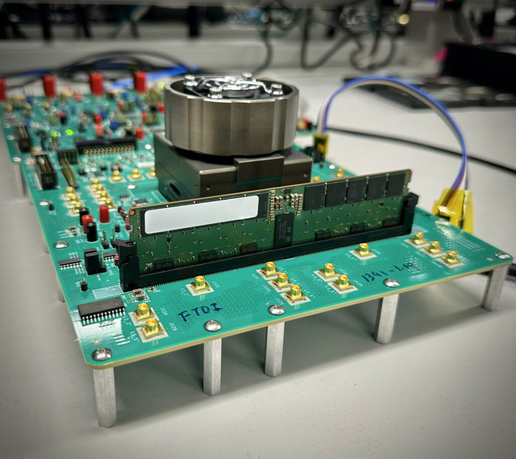
The Cadence DDR5 MRDIMM IP design is validated in hardware using the most recently available MRDIMMs (Gen2), reportedly achieving a best-in-class 12.8Gbps data rate that doubles the bandwidth using current DDR5 6400Mbps DRAM parts. (Image courtesy Cadence Design Systems, Inc./Business Wire)
Cadence is working to accommodate unprecedented AI processing demands.
SAN JOSE, Calif.—Cadence Design Systems recently introduced what it described as “the industry’s first DDR5 12.8Gbps MRDIMM Gen2 memory IP system solution on the TSMC N3 process.” The new system is reported to address the need for greater memory bandwidth to accommodate unprecedented AI processing demands in enterprise and data center applications, including AI in the cloud.
The Cadence® DDR5 MRDIMM IP offers a new high-performance, scalable, and adaptable architecture based on Cadence’s DDR5 and GDDR6 product lines. Multiple engagements are already underway with leading AI, HPC, and data center customers, the company stated in a release.
Data center and enterprise applications “stand to gain a significant performance advantage” from the DDR5 12.8Gbps MRDIMM IP system, according to the company. The new Cadence DDR5 IP offers a PHY and a high-performance controller as a complete memory subsystem. The design is validated in hardware using the most recently available MRDIMMs (Gen2), achieving a best-in-class 12.8Gbps data rate that reportedly doubles the bandwidth using current DDR5 6400Mbps DRAM parts.
The DDR5 IP memory subsystem is based on Cadence’s silicon-proven, high-performance architecture, ultra-low latency encryption, and RAS features. The DDR5 MRDIMM Gen2 IP is designed to enable advanced SoCs and chiplets with flexible floorplan design options. In addition, the new architecture allows fine-tuning of power and performance based on individual application requirements, the company said in the release.
“The Cadence DDR5 IP portfolio, together with Micron’s industry-leading 1γ (1-gamma)-based DRAM, meets the increasing demand for higher memory bandwidth, density, and reliability for AI processing workloads,” said Praveen Vaidyanathan, vice president and general manager of Micron’s Data Center Products, in the release. “These memory enhancements are pivotal in enabling the next generation AI/ML and HPC applications in data center and enterprise environments.”
Cadence’s DDR5 controller and PHY have been verified with Cadence’s Verification IP (VIP) for DDR to provide rapid IP and SoC verification closure. Cadence VIP for DDR5 includes a complete solution from IP to system-level verification with DFI VIP, DDR5 memory model and System Performance Analyzer.
“Data center and enterprise applications stand to gain a significant performance advantage from Cadence’s DDR5 12.8Gbps MRDIMM IP system solution, as evidenced by large customers turning to Cadence to deliver this innovative technology,” said Boyd Phelps, senior vice president and general manager of the Silicon Solutions Group at Cadence, in the release. “This new leading-edge memory IP system both raises the bar and establishes a roadmap that future-proofs our customers’ next-generation SoC and chiplet products for generations to come.”
Cadence describes itself as “a market leader in AI and digital twins, pioneering the application of computational software to accelerate innovation in the engineering design of silicon to systems.”
“Our design solutions, based on Cadence’s Intelligent System Design™ strategy, are essential for the world’s leading semiconductor and systems companies to build their next-generation products from chips to full electromechanical systems that serve a wide range of markets, including hyperscale computing, mobile communications, automotive, aerospace, industrial, life sciences and robotics,” the company stated in the release.