An example of a brazed assembly. (Image courtesy of Elcon Precision/The Partner Companies)
Elcon Precision and E-Fab offer expertise in processes that include photochemical etching, a fabrication method known to produce highly precise and durable thin metal parts.
By Mark Shortt
The Partner Companies (TPC) is a U.S.-based specialty manufacturing firm that produces mission-critical precision parts, components, and assemblies for essential industries. The company’s roots date back to 1997, when founders Dan Brumlik and Scott Bekemeyer set out to build a strategic ecosystem of specialty manufacturers.
The first company they acquired was Fotofab, a photochemical machining specialist in Chicago that manufactures precision metal-etched parts. Twenty-eight years later, TPC comprises 11 manufacturing companies—a global consortium of engineering and manufacturing capabilities for customers in the defense, aerospace, medical, telecommunications, semiconductor, and renewable energy industries.
The Partner Companies’ manufacturers specialize in niche processes, such as photochemical etching, ceramic metallization, crystal growth, and electropolishing. But its companies are also experts in core manufacturing capabilities like injection molding, machining, metal fabrication, and finishing, the company’s website stated.
Two of TPC’s companies, Elcon Precision and E-Fab, operate in close proximity to each other in Northern California’s Silicon Valley. According to TPC Group President Roy Barnes, Elcon and E-Fab embody the depth and breadth of TPC’s advanced manufacturing capabilities.
“OEMs and product manufacturers choose Elcon and E-Fab for their precise capabilities in photochemical etching, brazed assemblies, ceramic metallization, and the expertise of their in-house manufacturing teams that execute every step of these projects,” Barnes said in an emailed response to Design-2-Part. “Their manufacturing and engineering experts partner with customers to hone designs, technical specifications, and engineering plans to make every step of the manufacturing process run smoothly and efficiently.”
Elcon Precision, of San Jose, California, specializes in producing custom, metallized ceramic components and brazed assemblies. The company also manufactures vacuum coaxial switches and relays used by various defense contractors and systems integrators, Barnes said.
E-Fab, operating out of Santa Clara, California, specializes in producing thin metal parts, components, and assemblies using photochemical etching to deliver tight-tolerance, intricate parts at scale. The company manufactures parts such as antennas, electrodes, busbars, heat dissipation parts, circuitry, RF components, filters, and screens that integrators and contractors use in medical, communications, aerospace, and defense systems.
Both companies offer specialty expertise in photochemical etching (PCE), a fabrication method known to produce highly precise, durable, and reliable thin metal parts and components in a cost-effective manner. Their capabilities include working with several key materials, such as titanium, beryllium copper, stainless steel, molybdenum, Kovar, and tungsten. Each material requires a precise etching solution.
“Photochemical etching is a leading processing method to produce thin metal parts used in thousands of end products that save lives, help us communicate, and drive innovation,” Barnes said.
Barnes explained that photochemical etching is a precise subtractive manufacturing process that uses photolithography and chemicals to etch complex shapes and patterns into metal. The process begins with selecting and thoroughly cleaning the metal to remove contaminants before laminating it with a UV-sensitive photoresist. A UV laser digitally transfers the desired design onto the metal; after etching, the exposed resist is removed to reveal the pattern. The sheet is then rinsed and inspected.
“Photochemical etching enables the production of highly accurate, durable burr- and stress-free components with intricate geometries and tight tolerances—ideal for applications like surgical devices, semiconductor manufacturing, analytical instruments, electronic shielding, heat exchangers, and much more,” Barnes said.
The burr- and stress-free parts produced by photochemical etching come with no changes to material properties. Fast turnarounds and production times reduce lead times to days, rather than months. Cost-effective digital tooling is used, allowing for quick design changes and prototypes.
Ceramic metallization, brazed assemblies are key to bonding materials with thermal expansion mismatches
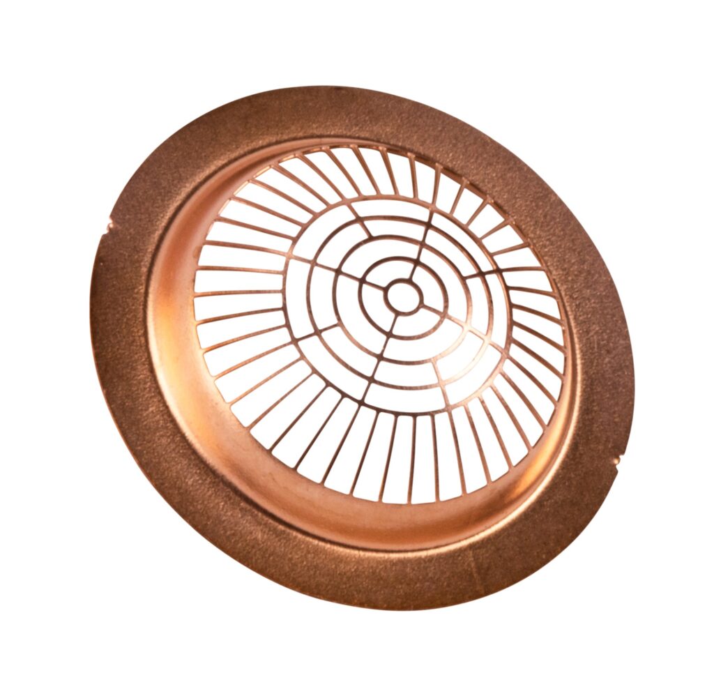
Three decades ago, Elcon Precision invented the process of etching and forming hemispherical grids. Today, the company specializes in manufacturing control and shadow grids for traveling wave tubes (TWTs), while continuing to “invest in new process equipment and inspection tools to meet increasingly tighter dimensions and tolerances on smaller and smaller parts,” Barnes said. Traveling wave tubes are microwave amplifiers that use hemispherical grids to control and focus electron beams. Systems that use TWTs include microwave receivers, communication satellites, and radar.
Elcon Precision recently collaborated with a customer in the defense industry to develop a critical component for a high-performance system that required exceptional thermal and electrical reliability. In its collaborative role, Elcon contributed its expertise in ceramic metallization, brazed assemblies, and final product testing. It also designed customer fixturing/tooling to assist with the brazed assemblies.
Barnes stated that Elcon could not disclose specific details due to the sensitive nature of the project. He noted, however, that the application demanded “stringent quality, durability, and hermetic sealing to ensure functionality under extreme conditions. ” The component required excellent thermal conductivity, electrical insulation, and robust bonding between ceramic and metal materials.
“There must be a guarantee that the manufacturing processes do not compromise base material integrity,” Barnes said. “Hermetic integrity and precise dimensional tolerances were critical to meet the demanding operational environment of the application.”
An example of a copper TWT grid. (Image courtesy of Elcon Precision/The Partner Companies)
One of the primary challenges was successfully brazing beryllium oxide (BeO), a material known for its excellent thermal properties but notoriously difficult to braze due to its thermal expansion characteristics. Achieving a strong, reliable bond to Invar while maintaining hermeticity and structural integrity under operating conditions posed a significant engineering hurdle, he said.
Elcon’s capabilities for providing ceramic metallization and brazed assemblies were key to overcoming this hurdle. Its team enhanced the bondability of the beryllium oxide by using its metallization process to create a durable foundation for brazing. Vacuum brazing was then employed to achieve a hermetic, high-strength bond between BeO and Invar, tailored to withstand the extreme performance requirements.
Elcon’s engineers also developed custom fixturing and tooling to stabilize the assembly during vacuum brazing, ensuring precise alignment and reducing thermal stress. “Our engineers also designed the process to manufacture these components with our technical services,” Barnes said.
Ultimately, comprehensive dimensional testing ensured precise tolerances. Hermeticity and electrical testing verified that the component met the rigorous specifications required for its application, he said.
Capabilities ranging from mesh screens to black oxide-coated optical parts and high-frequency laminate PCBs
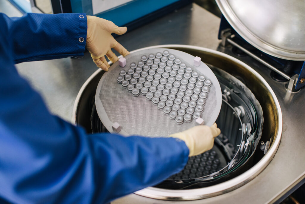
Both Elcon and E-Fab produce photochemically etched mesh screens for use in a wide range of applications, from medical devices and particle filters to hydraulic systems and current collectors. The companies customize products based on several factors, including material type, material thickness, and hole size, shape, and spacing.
“Holes are produced in a variety of geometries and tailored to meet the unique needs of the project,” Barnes explained. “Chemical etching of screens is a fast and inexpensive manufacturing method, with minimal tooling required for new or revised designs.”
E-Fab’s mesh screens are made from a solid piece of thin sheet metal. The company employs the photochemical machining process to manufacture “precision mesh screens that are durable and will not unravel,” according to Barnes.
Another E-Fab specialty is its production of black oxide-coated parts for optics. To create these parts, the company combines the precision of photochemical etching with advanced black oxide finishing.
“These parts enhance optical performance by reducing glare, controlling reflection, and providing a sleek, durable finish,” Barnes explained. “E-Fab’s black oxide parts are engineered to meet the high standards of industries like aerospace, defense, and precision instrumentation.”
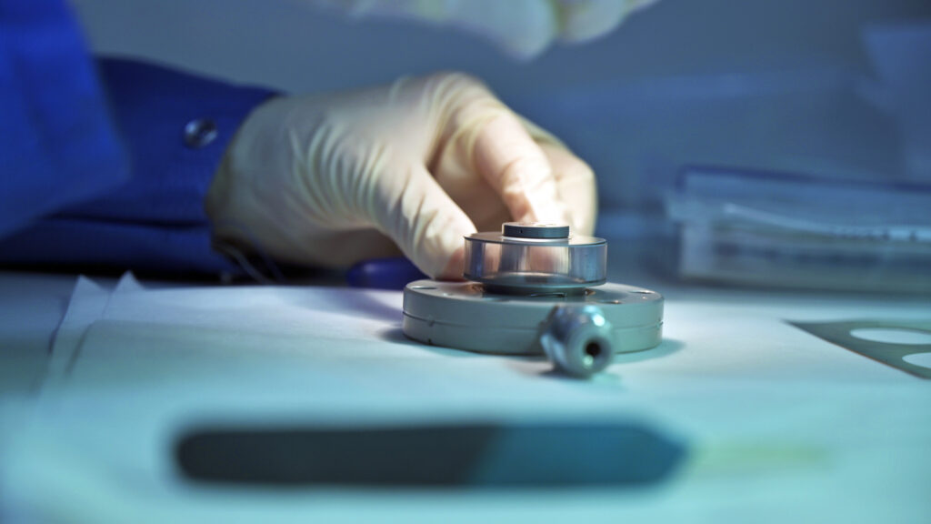
Metallized ceramic parts are placed into a furnace. (Image courtesy of Elcon Precision/The Partner Companies)
E-Fab’s capabilities also include the raw manufacturing of flex circuits, which allows E-Fab to build precision flex circuits, sculptured flex circuits, custom etched flex circuits, and hybrid circuit packages. In addition to fabricating microwave and RF printed circuit boards to customers’ prints, E-Fab also specializes in photochemical etching for high-frequency laminate PCBs.
“They are the backbone of a wide range of critical applications, especially in the defense and aerospace industries,” said Barnes.
The company also leverages its photochemical etching process to produce high-precision, highly customizable lead frames with intricate geometries, fine features, and exceptional consistency.
These parts are critical components in semiconductor packaging, as they provide the necessary electrical connection between the silicon chip and the external device.
An ecosystem of collaborative, integrated manufacturing companies
As constituents of The Partner Companies, Elcon and E-Fab are integrated with nine sister companies that complement their services and are able to step in if a part or component requires an additional manufacturing process. The TPC business model also provides geographic diversity, offering flexibility to customers while maintaining the same level of quality.
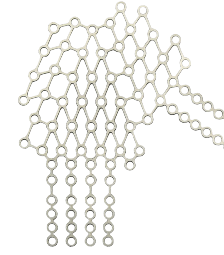
An example of a titanium surgical mesh. (Image courtesy of Elcon Precision/The Partner Companies)
“TPC combines entrepreneurial agility with the strength of an integrated manufacturing ecosystem,” Barnes said. “From the smallest component to full integration in complex assemblies, TPC’s operational agility enables customers to move from concept to implementation with consistent quality, precision, and efficiency across its companies.”
Besides Fotofab, Elcon Precision, and E-Fab, TPC’s companies also include Lattice Materials, Bozeman, Montana; L&T Precision, Poway, California, and Tijuana, Mexico; Microphoto, Roseville, Michigan; Optiforms, Temecula, California; Photofabrication Engineering, Inc. (PEI), Milford, Massachusetts; Pinnacle Precision, Anaheim, California; UPG, Houston, Texas, Suzhou, China, and Cardiff, Wales; and the most recent addition, Precision Eforming, a Cortland, New York-based manufacturer of precision electroformed parts (see The Partner Companies Acquires Precision Eforming).
Fotofab, Microphoto, and PEI provide photochemical etching and thin metal forming services for customers who need intricate parts that can be trusted to perform in diverse and complex environments. These companies serve the clean energy, medical technology, and aerospace and defense industries.
L&T Precision, Pinnacle Precision, and UPG offer manufacturing expertise in areas spanning injection molded plastic parts, sheet metal fabrication, precision machining, finishing, total integrated assembly, quality assurance, and more. Their capabilities support industries such as medical, data centers, energy systems, aerospace, and defense, as well as other commercial businesses, he said.
Lattice Materials and Optiforms manufacture optical components, including many for the defense industry. Lattice Materials custom grows silicon and germanium crystals used in mission-critical parts, while Optiforms provides electroformed and electroplated components, as well as thermal infrared components and thin-film optical coatings, according to the companies’ websites.